
An Investigation and Novel Development of High Efficiency, Low Cost CZTS Thin Film Solar Cells on Flexible Substrates
Project Leaders: D. Hodges
Research Goals: The fundamental scientific and engineering research in the design and realization of new electronic materials for thin film photovoltaics on flexible substrates is being investigated. A significant portion of this effort is devoted to developing, analyzing, and using special optical materials. Recently, the quaternary semiconductor Cu2ZnSnS4 (CZTS) has attracted a lot of attention as a possible absorber material for thin film solar cells due to its direct bandgap energy and high optical absorption coefficient. The objective of this project is the study and investigation of the transport and optical properties of CZTS. Next generation thin film photovoltaics (PV) need to achieve conversion efficiencies beyond 15%, and contain abundant and non-toxic materials with reliable and flexible modules, in order to succeed in the market in the long term. The scope of this present work will address fundamental issues related to design, fabrication, testing and characterization, including the basic science of the ability to control and modify structures, materials and thin film solar cell devices, addressing challenges in the formation of the stoichiometric, single phase kesterite, CZTS. The complete device structure, deposition techniques, layer thickness and processing direction is shown in Figure 1. CZTS thin films will be deposited by solution processing and spin coating, followed by annealing at temperatures ranging from 400°C to 600°C. The effect of annealing temperature on the formation of single phase CZTS can be seen in Figure 2, where additional phases develop at higher annealing temperatures. The challenge of maintaining stoichiometry of the CZTS thin films, as elemental constituents have high vapor pressures and can be lost during high temperature processing, is the formation of the correct kesterite crystalline phase. This project will study, fabricate and characterize CZTS solar cell devices, optimize processing conditions and studying the device performance based on the processing conditions. Temperature and atmosphere control during the annealing process is essential to control of the composition and crystal structure. In order to control the reactions during the annealing step, it is important to control temperature ramps and times, since too steep temperature ramps or too short annealing times can inhibit the formation of large grains. CZTS decomposition and binary losses must be prevented, while achieving the formation of large grains during annealing.
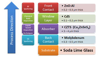
CZTS Solar Cell Device Structure and Process Direction
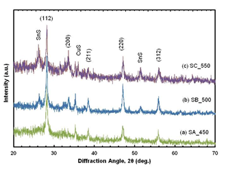
XRD profiles of CZTS thin films annealed at temperatures ranging from 450°C to 550°C, showing the development of additional phases at higher annealing temperatures.


